AUTOMATE COMPLIANCE CHECK
Given the intricate nature of semi-conductor designs, traditional and manual compliance checks are not only time-consuming but also prone to human error. Agile practices try to address this by bringing automation for compliancy and reliability checks into the design workflow.
Advantages of Automated Compliance Checks:
• Consistency and Accuracy: Automated tools can consistently apply compliance rules across all design stages, reducing the risk of overlooking critical issues.
• Fast Feedback: Designers receive fast feedback on compliance violations, allowing for prompt corrective actions without disrupting the overall workflow.
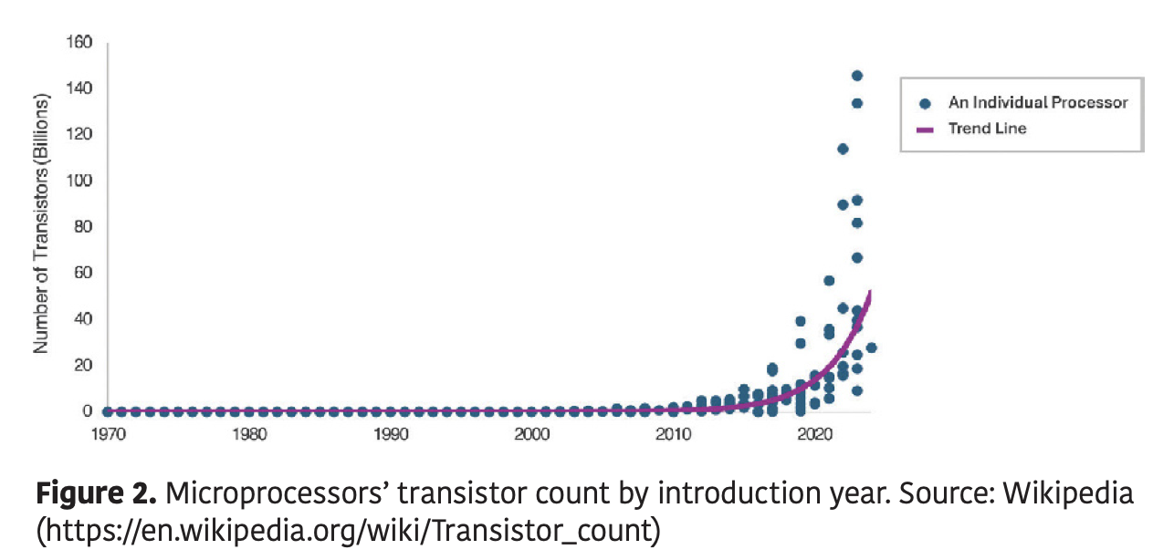
• Scalability: As designs grow incomplexity –for example, Figure 2 demonstrates the exponential increase in the number of transistors per CPU over the years– automated compliance checks can scale accordingly, handling larger datasets and more intricate rules without a proportional increase in effort.

To effectively automate compliance checks in chip design, leveraging advanced EDA (Electronic Design Automation) tools is essential. Modern EDA platforms offer comprehensive capabilities such as DRC (Design Rule Checking) and LVS (Layout Versus Schematic) verification. These tools automatically ensure that chip layouts comply with manufacturing constraints and industry standards, enhancing manufacturability and reducing the like likelihood of costly post-production errors. By integrating these advanced EDA tools into the Agile workflow, design teams can maintain high standards of compliance seamlessly throughout each iteration of the design process. In addition to EDA tools, advanced data analytics platforms play a crucial role in managing and analyzing the vast amounts of simulation data generated during chip design. Tools designed for big data analytics can process and interpret terabytes of data produced from FPGA (Field-Programmable Gate Array) prototyping, SoC (System on a Chip) emulation, oscilloscopes and logic analyzers. These analytics tools identify patterns, detect anomalies, and ensure that designs meet both functional and regulatory compliance requirements. By automating the analysis of complex simulation data, these platforms enable faster identification of potential compliance issues, allowing teams to address them early in the design cycle. Furthermore, specialized compliance automation solutions complement both EDA and data analytics tools by providing targeted verification and reporting capabilities.
These solutions ensure that many aspects of compliance are thoroughly checked and documented, facilitating easier audits and certifications. Integrating these diverse automation tools into an Agile framework ensures that compliance checks are not only thorough and efficient but also continuously aligned with evolving industry standards. Beyond advanced EDA and data analytics tools, a variety of specialized automation solutions could further enhance compliance verification in chip design. Take DRC tools as an example. These tools are essential for ensuring that chip layouts comply with manufacturing constraints. By employing automation, they could verify layout designs against predefined rules as part of the design process flow. This ensures manufacturability and reduces the likelihood of costly post-production errors. By investing in and integrating automation in the design flow, semiconductor design teams can ensure continuous adherence to industry standards and regulatory requirements. This enhances the reliability and quality of chip designs while accelerating the development process by minimizing manual interventions and reducing the likelihood of costly compliance-related revisions.
