Applying Agile and Lean Practices to Semiconductor Development
Introduction
The semiconductor industry is the cornerstone of modern technology, powering everything from smartphones and home appliances to automobiles and medical devices. Historically, semiconductor development has adhered to the waterfall model, characterized by sequential phases, rigid processes, extensive documentation, and prolonged lead times. While effective in certain contexts, this approach often struggles to keep pace with rapid technological advancements and dynamic market demands inherent to the modern semiconductor landscape.
Applying Agile and Lean principles and working methods to semiconductor development promises to address many challenges faced by traditional models, offering a pathway to more efficient, responsive, and innovative design processes.
The Traditional Waterfall Model
The waterfall model segments semiconductor development into distinct, non-overlapping phases:
1. Requirements Gathering: Defining specifications based on market/customer needs and considering technological capabilities.
2. Design Entry: Creating high-level architecture, followed by detailed microarchitecture and RTL (Register-Transfer Level) design.
3. Verification: Ensuring each component and the integrated system meet specifications through extensive simulations.
4. Physical Design: Translating logical representation of the circuit into fabrication ready design, involving layout, routing, and fabrication preparations.
5. Validation: Post-silicon testing to confirm operational parameters and performance metrics.
This linear progression can lead to bottlenecks, where delays in one phase cascade through the entire project. Additionally, the rigidity of the waterfall model makes it challenging to incorporate changes once development is underway, potentially resulting in products that lag behind evolving market demands and customer needs.

Four Key Principles of Agile Semiconductor Development
Drawing inspiration from the Agile Manifesto and adapting to the unique challenges of semiconductor development, the following principles guide an Agile approach to semiconductor development:
1. Functional Prototypes Instead of Comprehensive Complete Designs
The main advantage of Agile semiconductor design is in significantly reducing costs associated with verification and validation through iterative prototyping. The emphasis is on functional prototypes over striving for comprehensive complete designs from the outset. This approach fundamentally shifts the traditional paradigm of semiconductor design, where the goal has often been to develop a fully featured and complete model before moving forward in the development cycle.
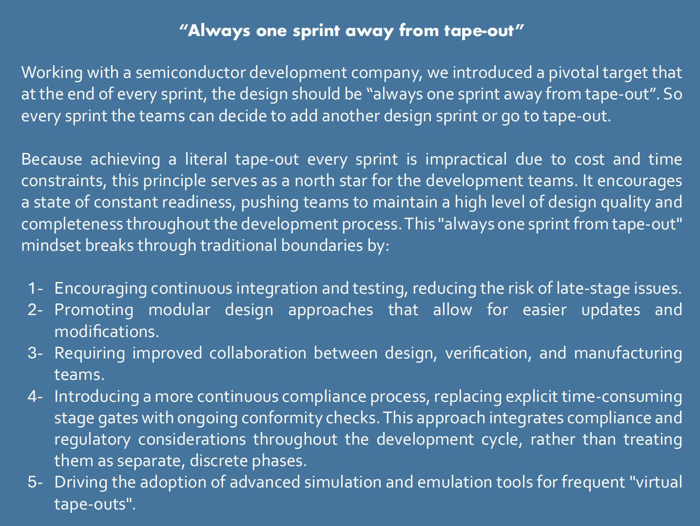
Instead of striving for a single, comprehensive design point, Agile semiconductor development focuses on creating tape-out-ready designs with minimal features. These prototypes serve as the foundation for adding features iteratively, ensuring that there is always a viable design available for deadlines. This approach not only mitigates the risk of overshooting and missing deadlines but also enhances verification by using tape-out-ready implementations for testing and feedback.
The focus is on iteratively adding features to the prototypes. Each prototype is a tape-out-ready design with a subset of the desired functionalities. This incremental approach allows designers to build upon a stable foundation, ensuring that each new feature integrates seamlessly with the existing design. By continuously refining and expanding the prototypes, the development team maintains a steady progression towards the final product without the need to overhaul the entire design for each new feature addition.

2. Multi-specialization Teams over Mono-specialization Teams
Traditional semiconductor design teams are often segmented into highly specialized silos, such as architects, RTL designers, analog designers, mixed-signal designers, layout engineers, verification engineers, and test engineers. This compartmentalization can lead to significant communication overhead and potential misunderstandings, as each specialized group focuses narrowly on their specific tasks without a comprehensive view of the entire project. The reliance on extensive documentation to bridge those silos not only slows down the development process but also increases the risk of errors and misalignments between different stages of the design cycle.
In contrast, Agile development advocates for multi-specialization teams that are capable of handling features end-to-end and through all stages. These teams create a collaborative environment where engineers develop a T-shaped skillset, combining deep expertise in one area with broad capabilities across multiple disciplines. This versatility allows team members to communicate effectively and contribute to various aspects of the design process, from initial architecture to final verification and testing. Additionally, focusing on feature implementation within a unified team structure –instead of focusing on cross-silo communication– ensures that all members are aligned with the project’s goals and changes, leading to more cohesive and efficient workflows. This approach not only streamlines the design process but also empowers engineers to adapt more readily, ultimately resulting in higher-quality silicon delivered in shorter timeframes.
This multi-specialization approach can be particularly beneficial in bridging the gap between digital and analog design teams, as well as between design and verification teams. This integration can lead to more holistic designs and more efficient problem-solving, further supporting the goal of maintaining tape-out readiness at all times.
3. Advancing Tools and Generators over Refining Instances
IC design toolchains are traditionally less automated and more rigid compared to software development environments. Investing in advanced hardware description languages (HDLs) and automated physical design flows is essential. Agile semiconductor development emphasizes the creation of highly parameterized hardware generators and the improvement of HDLs to enable reuse and automation. By investing in more sophisticated HDLs, engineers can create reusable and adaptable components easier. Also, this would enable them to explore diverse design spaces without the need for extensive manual modifications. This shift from refining individual instances to developing robust generators enable teams to efficiently iterate on designs and incorporate new features with ease.
Moreover, automation plays a pivotal role in reducing the reliance on manual interventions within the build process. Agile practices advocate the development of automated physical design flows, which streamline tasks such as synthesis, layout, and timing analysis. By minimizing manual steps, these automated processes not only enhance productivity but also reduce the potential for human error.
Additionally, incorporation of reusable verification infrastructures ensures that each design iteration undergoes consistent testing, further lowering verification costs and accelerating the development cycle. This focus on improving tools and generators allows designers to concentrate on innovation and creative problem-solving, rather than being bogged down by repetitive tooling issues and manually fiddling with CAD designs, ultimately leading to more efficient and higher-quality semiconductor products.
This principle can be extended to the development of IP blocks by parameterizing them and creating reusable design components and platforms. This approach not only makes it easier to apply changes throughout the design process; but also improves consistency and reliability across different designs, supporting the goal of maintaining tape-out readiness throughout the development process.
4. Responding to Change over Following a Plan
While semiconductor designs are eventually translated into mask sets ready for fabrication, Agile methods embrace change in their specifications during the development phase. This flexibility allows teams to adapt to evolving market conditions, feature requests, or updates to industry standards by treating changes as feature reprioritizations/introduction. Prioritizing the implementation of core features and specification that are unlikely to change, reduces the risk of wasted effort due to later design changes and enhances the overall adaptability.
Also, incorporating set-based design principles further enhances this adaptability by keeping multiple design options open throughout the development process. Set-based design involves exploring a variety of design alternatives in parallel, allowing teams to evaluate and refine different approaches before converging on the most optimal solution. By maintaining a diverse set of viable design pathways, teams can swiftly pivot and integrate new features or modifications without significant rework.
One way to apply this is through the use of reconfigurable hardware platforms like FPGAs for early prototyping and validation. This allows teams to test and refine designs before committing to a final design, supporting the goal of maintaining tape-out readiness while allowing for flexibility in design choices.
Conclusion
The adoption of Agile practices in semiconductor development represents a paradigm shift from traditional, rigid processes to more flexible, iterative, and collaborative approaches. By embracing principles such as incremental prototyping, continuous verification and crossfunctional teamwork, semiconductor design companies can enhance efficiency, reduce costs, and foster innovation. The successful implementation of Agile practices has the potential to transform the semiconductor design sector, ensuring that it remains responsive to the rapid technological advancements and dynamic market demands of the modern era.
References
- J. N. Allen, H. S. Abdel-Aty-Zohdy and R. L. Ewing, "Agile Hardware Development with Rapid Hardware Definition Language," 2009 IEEE International Conference on Electro/Information Technology, Windsor, ON, Canada, 2009, pp. 383-388
- Y. Iwata, K. Taji, and H. Tamura, “Multi-objective Capacity Planning for Agile Semiconductor Manufacturing,” Production Planning & Control, vol. 14, no. 3, pp. 244–254, Apr. 2003
- Y. Lee et al., "An Agile Approach to Building RISC-V Microprocessors," in IEEE Micro, vol. 36, no. 2, pp. 8-20, Mar.-Apr. 2016
Highberg, a consulting firm with over six years of experience in the semiconductor industry, has been at the forefront of implementing Agile and Lean practices in this sector. Working with some of the industry's top companies, Highberg has demonstrated the power of these practices in improving semiconductor development processes. Key benefits include significantly reduced time-to-market, enhanced adaptability to changing market demands, and overall improvement in product quality. Additionally, clients experience increased team collaboration and more efficient resource utilization. Highberg's expertise in tailoring Agile and Lean practices to the unique challenges of semiconductor development has made them a valuable partner for companies seeking to stay competitive in this rapidly evolving industry.
Want to know more?
Get in touch today!